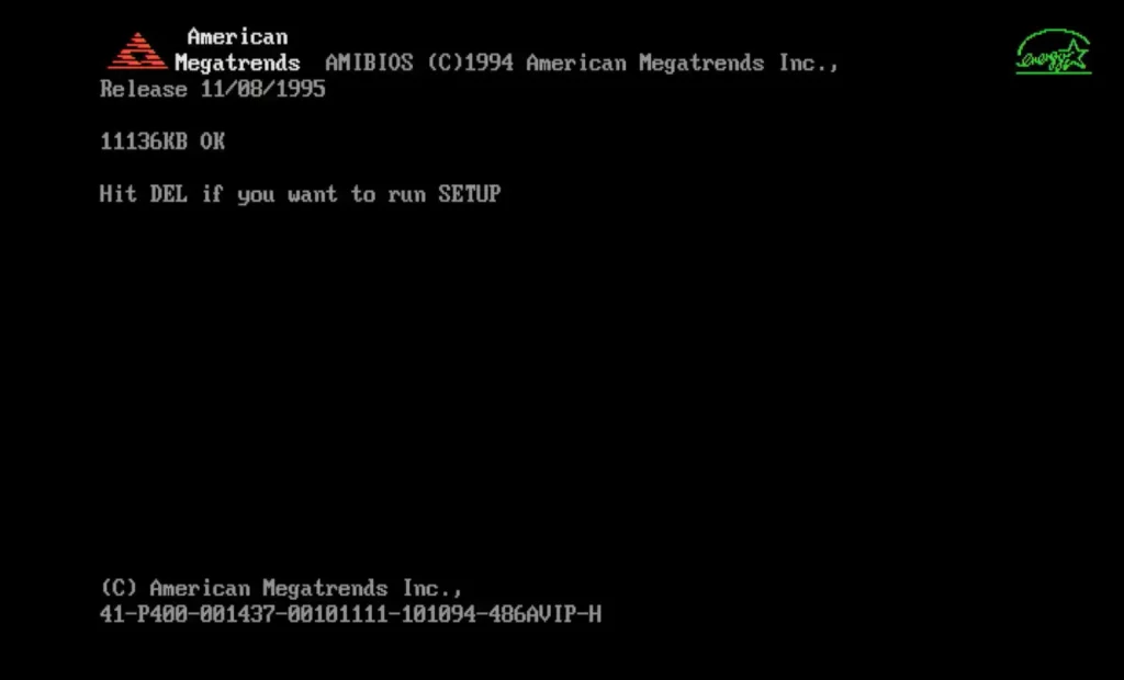
I am not here to insult your Socket 3 motherboard – if you are the owner of this specific model and love it: The PCChips M915i. I recently had this board in for “repair”, even though it is supposed to be “new old stock” (NOS). Luckily, nothing was at fault! All it needed was FPM memory instead of EDO. My suspicion is that the owner tried to run the board with EDO memory – and that will prevent the board to POST. (If you are looking for the BIOS image with the FAKE CACHE mod, scroll to the end).
The memory wasn’t the only issue I discovered. The board also had fake cache chips soldered to the board. OK, not the first time I came across this shady practice of early motherboard manufacturers and distributors. Removing those old DIP cache chips isn’t that difficult if you’re not forced to use solder wick or a desoldering station. Hot air is my preferred choice; However, in this case, the DIP chips started to melt at a temperature of around 200 degrees – that shouldn’t happen! Well, as it turns out, the cache chips consist of cheap plastic bodies that cannot withstand the heat. You can see all this in the video.
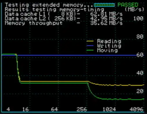
Unfortunately, replacing the fake cache chips with real cache chips wasn’t enough. The cache still doesn’t work. With 256K of L2 cache installed, no gains can be seen in SpeedSys. If the cache would operate, we should see a drop at 256K as well. Not as prominent like we see at 8K, but there should be a visible drop in the graph.
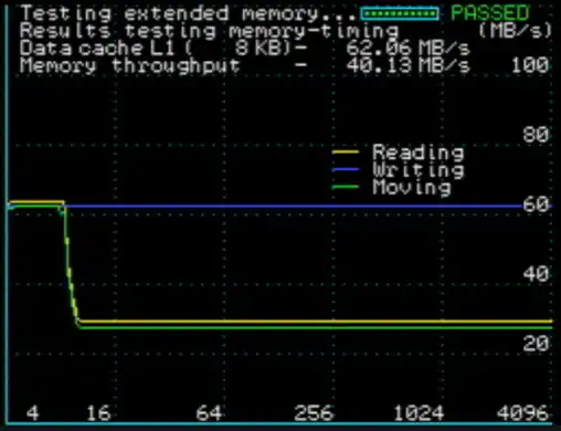
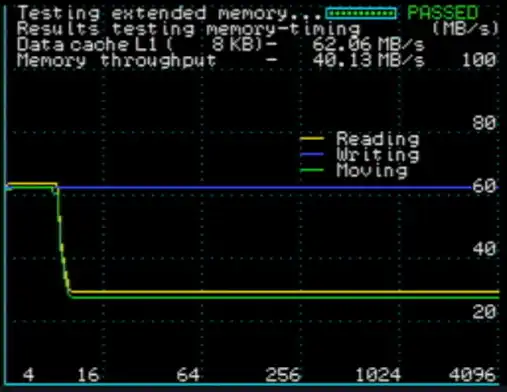
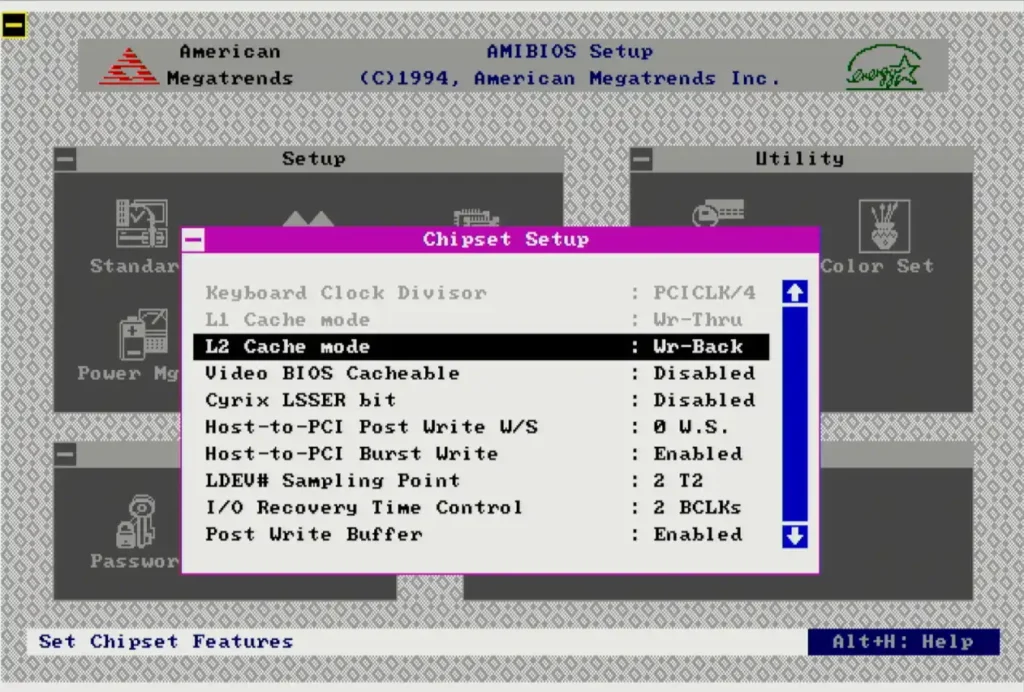
Both graphs (left Write-Through, right Write-Back) show the same results. It looks like the BIOS doesn’t know how to utilize the newly installed cache. The confusing part is that all options to control the cache are available configurable in the BIOS.
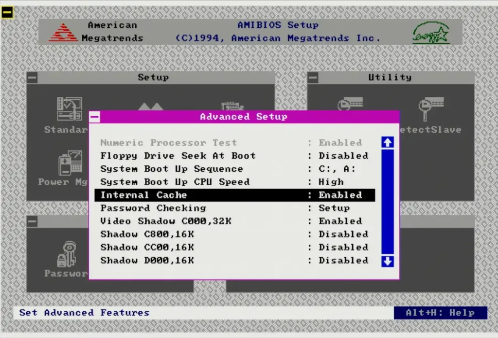
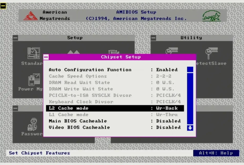
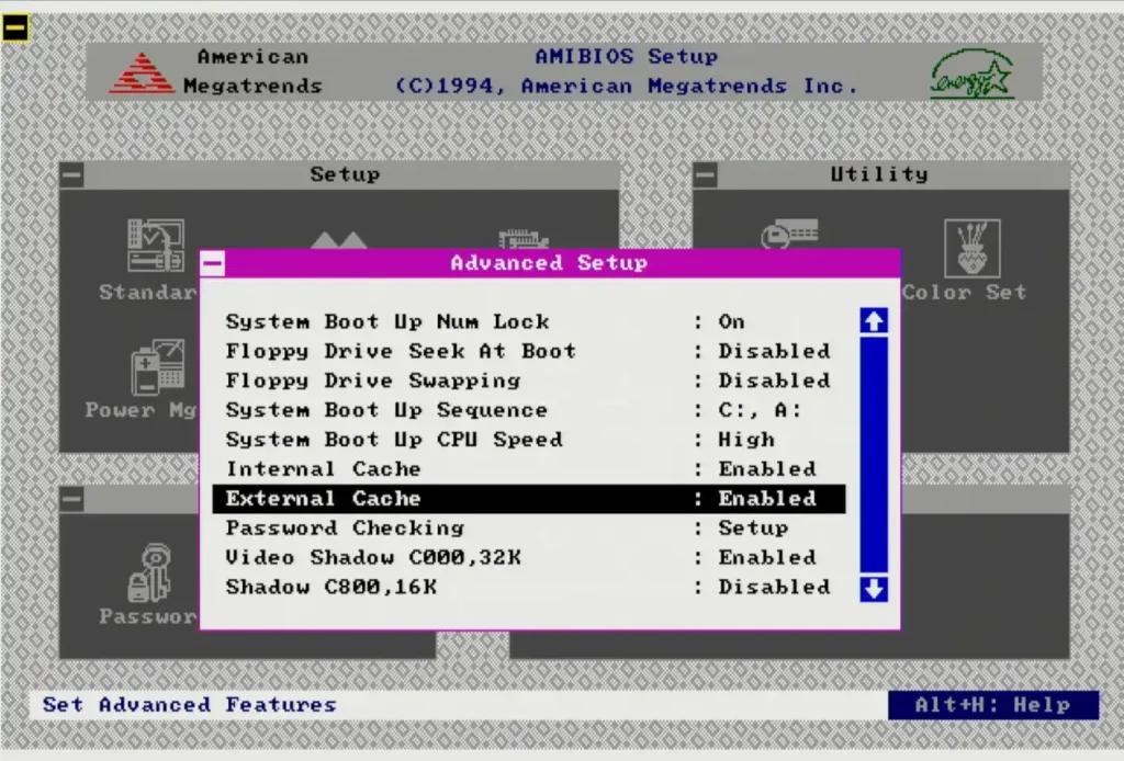
The BIOS doesn’t allow us to ENABLE/DISABLE the L2 cache, but it does have a setting in the “Chipset Setup” that allows us to change between Write-Back and Write-Through. The results of this setting don’t affect the performance in any way because the board simply doesn’t utilize the installed cache memory. Not only does this BIOS always report 256KB of L2 cache (no mater what is installed), it also doesn’t utilize the the cache if it is actually installed on the board.
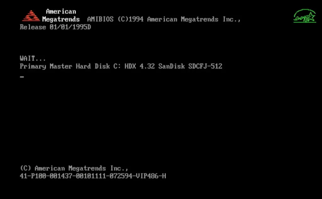
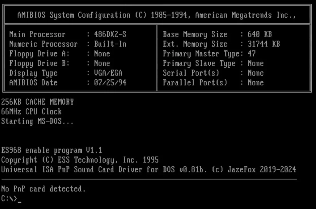
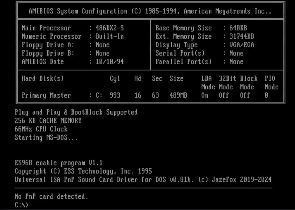
The release date of the board is mentioned as “01/01/1995D” and it reports 256KB CACHE MEMORY. But usable is 0K.
The Retro Web has two newer BIOS versions for download. Both have a date code of 11/08/1995, but one adds the suffix “S”. We will test both versions and determine which one is the better one. Since my board had a One-Time-Programmable BIOS chip, I had to replace it with a SST29EE010 128K chip. This chip seems to be compatible with the board.
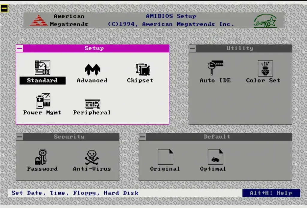
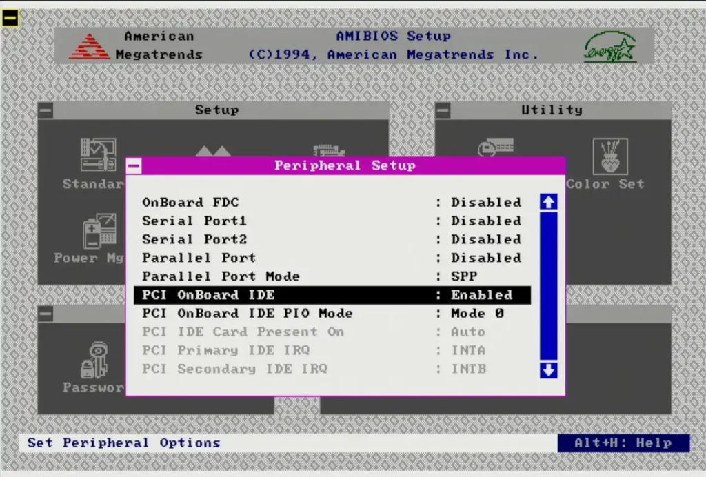
The newer BIOS definitely has some upgrades in the UI! IDE auto detection has combined Primary and Secondary IDE channels and we get a new “Peripherals” option under setup.
The optimized UI is not the only change – we now get an option to ENABLE/DISABLE the Level 2 cache! Maybe this option was disabled in the original BIOS and not shown to the user to enable it. They knew that there was fake cache on the board and the option would be useless. Nobody would desolder the chips anyway and look closer, right? Other than providing an option to enable and disable the L2 cache, we get the option of setting L2 cache to Write-Through and Write-Back mode. The question is – does the L2 cache work now by just updating the BIOS?
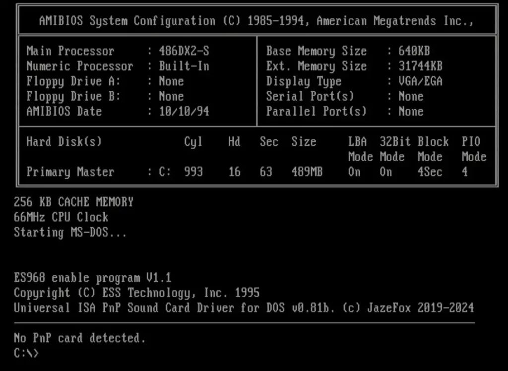
Before we test the cache, I’d like to show you the new “Peripherals” feature. Did I mention that this board does not have a floppy drive controller? It also doesn’t have COM ports or a parallel port (LPT, printer port). I guess you are supposed to get a controller card if you need those ports. We should disable all but the OnBoard IDE ports.
The big question is – does the cache work with the new BIOS?
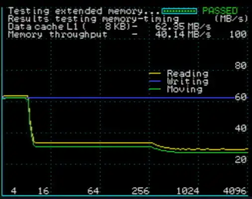
On the left is the Write-Through L2 cache and on the right we can see how the performance changes when we configure the L2 cache as Write-Back. Interesting is that the memory through decreases in Write-Back mode. That might be due to the CPU which operates in Write-Through. The DX2 from Intel was released in two versions. One could only operate in Write-Through, while an updated version could also operate in Write-Back mode. The point is – the CACHE IS WORKING!
I tested both version available on The Retro Web – on the left is the regular “11/08/1995”, while on the right is the one with suffix “S”.
Compared to the BIOS which always shows “256KB CACHE MEMORY”, the BIOS versions that work correctly with cache have a space between the numeric value and “KB”. So, it says” 256 KB CACHE MEMORY”. Furthermore, we get more information of our attached IDE hard drives (ignore the PIO mode, I think I forgot to configure this for the “S” BIOS). An interesting addition to the “S” version of the BIOS is that it seems to support “Plug and Play & BootBlock Supported” – that is interesting! So, are we be able to use a tool like Uniflash now to update the BIOS? If you watch my video, you will see that all the tools I tried refused to work with the original BIOS chip.
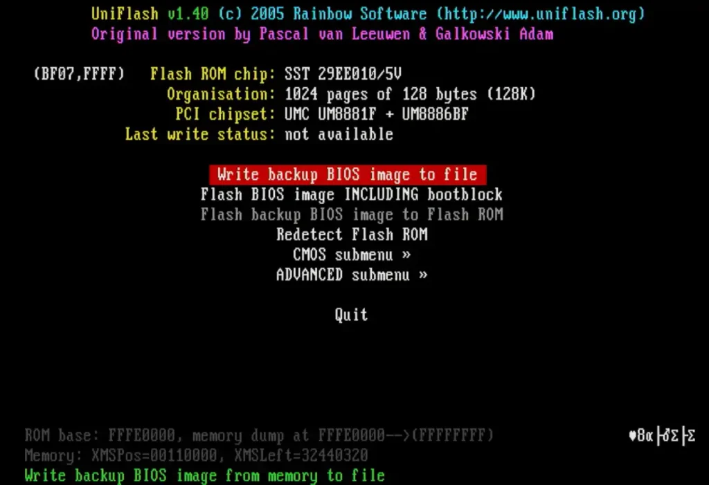
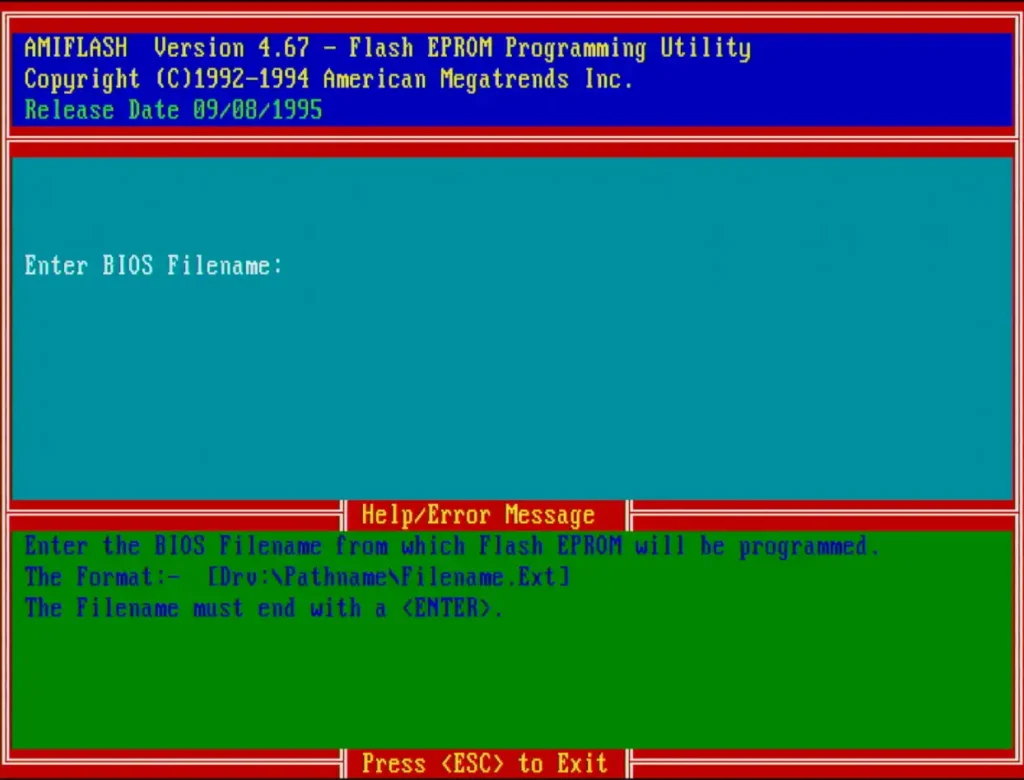
YES! Both tools, UniFlash as well as AMIFLASH seem to detect the SST29EE010 and allow us to flash the BIOS if we wanted to. But, it is safe to say that most likely, there aren’t going to be any new BIOS version released for this board.
But there is more about this board, but for this you need to watch the video on YouTube – you won’t believe how I found out the the RTC chip has a reversed pinout…
And finally – for those who would like to check the patched BIOS with non-working cache support an which always reports 256KB CACHE MEMORY is installed, here is the file. I tested the file by flashing it to the same SST29EE010 – so, I am pretty confident that this is the copy of the One-Time-Flash chip. I had to copy 64K segments together that were extracted from different tools, but it seemed to have worked. Thanks for reading and I hope you enjoyed this project! Leave me a comment on my video and don’t forget to like and subscribe!